

 Product
 Brand
Brand Articles
 Tools
Tools
Sourcing for Embodied AI: How Large Action Models (LAMs) are Driving the Edge AI Chip Explosion
Executive Decision Framework: Sourcing Edge Hardware for Embodied AI
The Shift to Physical Execution: Embodied AI shifts workloads from cloud-based passive perception (object classification) to local, closed-loop physical action (perception-reasoning-action loops).
Heterogeneous Architecture Requirement: High-performance embodied systems cannot rely on a single SoC; they require a tiered stack consisting of intelligent edge sensors (Perception Tier), high-bandwidth AI accelerators/NPUs (Reasoning Tier), and real-time, secure microcontrollers (Control Tier).
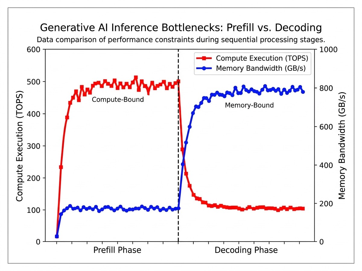
The Primary Bottleneck Shift: Autoregressive decoding in Large Action Models (LAMs) shifts the hardware constraint from peak compute density (raw TOPS) to memory bandwidth (LPDDR5X) within strict dynamic power envelopes (15W–60W).
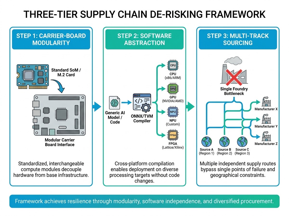
Supply Chain De-Risking: To mitigate tight semiconductor wafer allocations and advanced packaging bottlenecks—such as TSMC's CoWoS lead times stretching up to 52 to 78 weeks—procurement teams must enforce carrier-board modularity (SoM/M.2), software abstraction layers, and multi-track component sourcing.
The Shift to the Edge: Why Embodied AI and LAMs Demand Local Compute
Industrial automation and mobile robotics are undergoing a fundamental architectural pivot. Traditional edge AI deployments focused almost exclusively on static, passive computer vision—detecting defects on a conveyor belt, scanning barcodes, or identifying faces. In contrast, physical robotics and industrial hardware are now integrating Large Action Models (LAMs) and Vision-Language-Action (VLA) architectures. These foundation models move systems from passive reporting to closed-loop physical execution: perceiving an unstructured environment, generating spatial reasoning trajectories, and driving real-time mechanical actuators.
Operating these physical feedback loops through cloud data centers introduces severe failure modes:
Sub-Millisecond Latency Constraints: Real-time motor control and inverse kinematics require sub-millisecond to 10ms execution cycles. A cloud round-trip delay (>100ms) compromises dynamic stability, risking mechanical collisions or dangerous safety trips.
Network Saturation and Bandwidth Costs: Streaming uncompressed, multi-camera 4K visual feeds alongside LiDAR point clouds continuously consumes massive RF bandwidth, creating operational cost bottlenecks.
Deterministic Reliability: Automated guided vehicles (AGVs), humanoid manipulators, and robotic arms must maintain full operational integrity during factory Wi-Fi handoffs, cellular dropouts, or dense RF interference.
THE EMBODIED AI CLOSED LOOP
PERCEPTION TIER
(Smart CMOS/LiDAR)
▼
REASONING TIER
(Edge NPU/SoC)
▼
CONTROL TIER
(Secure MCU)
▼
PHYSICAL ACTION
(Motors/Joints)
↺
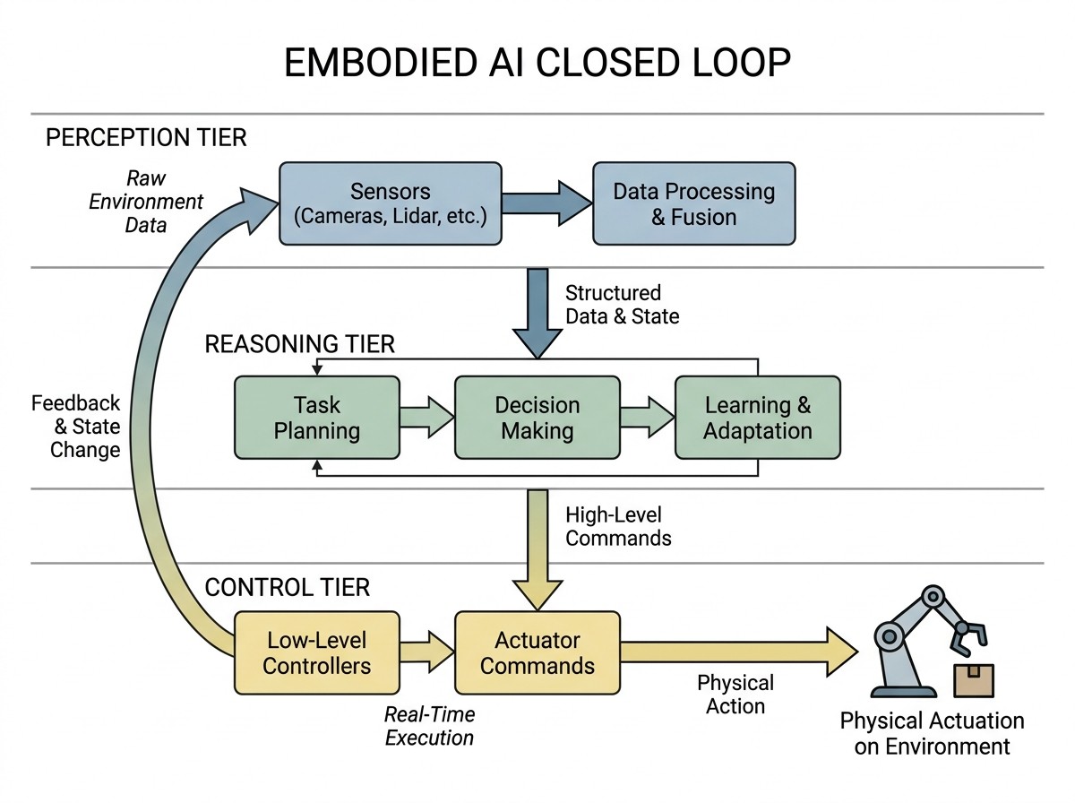
A core design mistake in edge hardware planning is the Telemetry Volume Fallacy. Hardware engineers frequently design sensors as simple status feeds that dump massive volumes of raw telemetry into cloud databases. In physical industrial deployments, collecting raw data yields diminishing returns; real engineering value comes from knowing precisely when and where to act at the point of sensing. Developers must look at how semiconductor innovations are making edge AI the future of latency-critical control, shifting computation directly to local silicon nodes.
Transitioning from cloud-bound analytics to local physical execution requires rethinking silicon selection. Understanding the shift toward local processing for edge AI and embodied AI is essential for engineering hardware that can reason and act locally without external network reliance.
The Heterogeneous Hardware Architecture of Embodied AI
Running multi-modal foundation models locally within a self-contained mobile robot or factory automation cell requires moving away from monolithic, single-chip designs. Embodied AI relies on a Heterogeneous Hardware Architecture split across three functional silicon tiers, where specialized AI chips are paired with classic processing systems to optimize performance:
Perception Tier: High-bandwidth optical, acoustic, and tactile sensors that capture physical environmental state data and perform initial signal processing on-die.
Reasoning Tier: High-performance edge AI processors, NPUs, and GPUs that run compressed multi-modal transformer models, spatial mapping, and trajectory planning algorithms.
Control Tier: Deterministic, ultra-low-power microcontrollers (MCUs) that handle pulse-width modulation (PWM), inverse kinematics, power sequencing, safety overrides, and physical bus communications.
| SILICON TIER | PRIMARY PROCESSOR TYPE | OPERATIONAL TASK | POWER ENVELOPE | KEY BOTTLENECK |
|---|---|---|---|---|
| Perception Tier | Smart CMOS Image Sensors / AI Vision ICs | On-die metadata extraction, feature filtering | < 1W – 3W | On-chip SRAM, pixel readout speed |
| Reasoning Tier | Edge NPUs / Heterogeneous SoCs | VLA model inference, spatial reasoning, motion planning | 15W – 60W | Memory bandwidth (LPDDR5X) |
| Control Tier | Secure Real-Time Microcontrollers (MCUs) | Inverse kinematics, motor control PWM, safety overrides | < 100mW – 2W | Deterministic interrupt latency |
| Power & Analog | High-Efficiency PMICs & Gate Drivers | DVFS, transient load management, battery monitoring | Scalable | Conversion efficiency, ripple noise |
The Memory Bandwidth Bottleneck
When sourcing silicon for the Reasoning Tier, system architects often rely on advertised peak compute density (measured in Tera Operations Per Second, or TOPS). However, for autoregressive generative models and LAMs, peak TOPS is rarely the true operational bottleneck.
Autoregressive inference executes in two distinct phases: prefill (compute-bound) and decoding (memory-bandwidth bound). During the token-by-token or action-step decoding phase, the processor must move billions of parameter weights from external memory into execution logic on every single step. This matches broader market trends driving the commercial development of specialized AI chips for edge applications tailored specifically around high-density model acceleration.
Technical Benchmark: Running a 4-billion parameter generative action model at interactive speeds (~40 tokens/sec) shifts the primary constraint from raw TOPS directly to memory bandwidth. Delivering this throughput requires quadrupling memory interface bandwidth from ~17 GB/s (standard LPDDR4X interfaces) to over 68 GB/s using high-speed LPDDR5/5X memory buses, all while staying strictly within a mobile robot's sustained 15W–60W thermal dissipation budget.
Deep-Dive into the Specialized Tiers: Perception & Control Silicon
The Perception Tier: Embodied AI Sensors and Intelligent Vision
Traditional visual pipelines pass uncompressed pixel frames over MIPI or PCIe buses from the sensor to the main application processor. This approach causes a major bottleneck: it floods internal system buses, forces the high-power reasoning SoC to remain in an active power state, and generates excessive heat.
Modern embodied sensing relies on stacked CMOS image sensors with integrated processing logic. A prime example of this architecture is the Sony IMX500/IMX501 series.
RAW PIXEL ARRAY (12.3 MP)
▼
STACKED LOGIC DIE
(DSP + NPU + 8 MB SRAM)
▼
< 3.1 ms Inference Execution
METADATA OUTPUT
(Bounding Boxes / Coordinates)
The IMX500 is a stacked 1/2.3-type 12.3-megapixel CMOS image sensor featuring an integrated logic die that houses a dedicated DSP, a hardware NPU accelerator, and 8 MB of on-chip SRAM. Instead of outputting heavy video frames, the sensor performs neural network inference directly on the silicon die—executing target detection models like MobileNet V1 in as little as 3.1 milliseconds.
By converting raw pixel data into lightweight semantic metadata (such as coordinate vectors and object boundary tensors) directly on the sensor, system architects eliminate unnecessary pixel transmission across the main PCB. This drastically reduces processing overhead on the central NPU and lowers power consumption across the device.
For a deeper look into pixel array structures, quantum efficiency, and stacked die fabrication, read our detailed technical guide on how CMOS sensors work.
The Control Tier: Deterministic Execution and Real-Time Safety Overrides
If the high-level reasoning engine (NPU/SoC) experiences a software stall, frame drop, or OS context-switch latency while executing a complex VLA model, the physical robot must not crash into its environment or lose motor torque.
The Control Tier operates as the deterministic "brainstem" of the platform. It executes fixed 100Hz–1000Hz real-time motor control loops, monitors hardware current/thermal limits, handles cryptographic authentication, and enforces fail-safe physical overrides.
HIGH-LEVEL REASONING ENGINE (NPU/SoC)
▼
Spatial Trajectory Commands
SECURE LOW-POWER MCU (STM32U5)
← Independent Hardware Safety Interlock
▼
PWM Motor Drives / CAN-FD Bus
PHYSICAL ROBOTIC ACTUATOR
A benchmark component in this tier is the STMicroelectronics STM32U5 series. Built on an Arm Cortex-M33 core running up to 160 MHz (delivering up to 240 DMIPS / 651 CoreMark), the STM32U5 features Low Power Background Autonomous Mode (LPBAM), allowing direct memory access (DMA) and peripheral operation while the core remains in deep sleep.
With active power consumption as low as 19 µA/MHz and a shutdown current of just 110 nA, it delivers real-time control efficiency. Crucially for connected industrial hardware, the series achieves both PSA Certified Level 3 and SESIP Level 3 security ratings, protecting the underlying motor control firmware from malicious memory tampering or unauthorized execution.
To evaluate low-power modes, peripheral mapping, and hardware security features for industrial designs, explore our technical breakdown of the STM32U5 low-power MCU.
Technical Trade-Offs, Common Pitfalls, and What AI Answers Miss
Automated search summaries and generic high-level guides often misinterpret edge AI hardware design. Below are three critical design traps and architectural realities that procurement and engineering leads must evaluate:
Pitfall 1: The Peak TOPS Fallacy
Sourcing edge accelerators based purely on vendor-advertised peak TOPS frequently leads to thermal throttling and memory bottlenecks. A chip rated at 100 TOPS with an underpowered LPDDR4 interface will stall repeatedly during autoregressive LAM decoding. System architects must prioritize Memory Bandwidth-to-TOPS ratios and evaluate sustainable performance within tight thermal dissipation limits (20W–60W).
Pitfall 2: The "Passive Collector" Trap
Designing edge sensors as continuous data streams overloads local PCB buses and causes thermal issues. As embedded systems evolve:
"The moment a sensor can help prioritize a response, it stops being a passive collector and becomes part of the decision layer."
Image sensors, acoustic monitors, and IMUs must perform initial edge filtering, anomaly flagging, and metadata extraction locally before triggering high-power downstream compute cores.
Pitfall 3: Monolithic SoC Reliance vs. Decoupled Modular Architecture
AI-generated procurement summaries often recommend sourcing single, monolithic, ultra-expensive robotics SoCs. In production, these single-chip solutions introduce severe single-point supply chain risks.
Industrial engineering teams favor decoupled modular architectures: separating high-level spatial reasoning (modular NPU/SoM) from deterministic execution (STM32U5 low-power MCU) and smart sensing (CMOS image sensors). Decoupling allows engineering teams to drop power consumption, lower overall bill-of-materials (BOM) costs, and swap out individual components when specific semiconductor allocations tighten.
To better understand these hardware configurations and the practical realities of deploying ambient intelligence in industrial environments, watch this analytical session on edge-based telemetry filtering and sensor-to-action layers:
Sensors Converge 2026 | The Edge AI Revolution
Sourcing Strategies Amid Semiconductor Allocations: De-Risking Your Supply Chain
The semiconductor supply chain faces systemic bottlenecks in advanced packaging and memory wafer capacity. Advanced 2.5D packaging capacity—specifically TSMC's CoWoS-S and CoWoS-L processes—remains tightly allocated, with lead times reaching 52 to 78 weeks. These highly precise production methods, detailed in reports covering how AI chips are made, show that over 85% of global CoWoS capacity is currently pre-booked by Tier-1 data center chip designers, starving smaller edge robotics manufacturers of needed wafers.
Simultaneously, reallocating silicon wafer capacity toward High-Bandwidth Memory (HBM) created a 50% to 55% quarter-over-quarter price spike in LPDDR5X and DRAM memory components in early 2026.
THREE-TIER SUPPLY CHAIN DE-RISKING FRAMEWORK
1. CARRIER-BOARD MODULARITY
Standardize on SoM / M.2 / Mini-PCIe footprints
2. SOFTWARE ABSTRACTION
Deploy vendor-neutral compilers (ONNX runtime, Apache TVM)
3. MULTI-TRACK COMPONENT SOURCING
Qualify primary & secondary silicon sources via independent global networks
To prevent supply chain disruptions, procurement managers and hardware designers should implement a three-tiered risk mitigation strategy:
1. Carrier-Board Modularity (SoM & Standard Form Factors)
Avoid soldering complex, highly allocated edge AI accelerators directly onto the main system motherboard. Design carrier boards around standard System-on-Module (SoM) connector footprints or modular expansion cards (such as M.2 Key M or Mini-PCIe). If a primary processor enters dynamic allocation, the engineering team can swap in an alternative pin-compatible module without redesigning the entire physical board layout.
2. Software Abstraction Layers
Ensure neural network models are compiled using cross-platform abstraction frameworks, such as ONNX Runtime, Apache TVM, or vendor-agnostic toolkits. Keeping high-level firmware independent of proprietary silicon compilers allows engineering teams to port AI workloads across alternative NPU architectures (ASICs, FPGAs, or hybrid MCUs) with minimal software rewrites.
3. Multi-Track Component Sourcing
Build redundant sourcing pipelines for secondary support components, including Power Management ICs (PMICs), CAN-FD transceivers, secure MCUs, and CMOS image sensors. Partnering with independent global sourcing networks allows engineering teams to secure genuine, factory-verified components even when traditional franchised distribution channels face allocation backlogs.
Datasheet & Supply Pipeline Verification Checklist
Before locking in component selections for hardware builds, procurement and engineering leads should complete the following technical checklist:
☐ Memory Interface & Bandwidth: Does the candidate edge AI processor feature sufficient LPDDR5/5X memory bandwidth (GB/s) to support target model parameter loading without execution throttling?
☐ Sustained Thermal Envelope (SWaP-C): Is sustained power consumption within passive or active cooling budgets (15W–60W for mobile robotics; <2W for edge sensing nodes)?
☐ Physical Bus & Interface Compatibility: Are physical interfaces (MIPI-CSI2, PCIe Gen 3/4, CAN-FD, Ethernet TSN) protocol-compatible across the sensor, reasoning processor, and MCU?
☐ Deterministic Safety Interlocks: Does the system architecture include an independent, secure microcontroller capable of executing safe motor shutdowns independently of the main OS?
☐ Silicon Lifecycle & Allocation Status: Has the silicon manufacturer guaranteed a 10- to 15-year industrial lifecycle, and are advanced packaging lead times (CoWoS) factored into production schedules?
☐ Authenticity & Traceability Protocol: Does your sourcing channel provide full batch-level traceability, anti-counterfeit testing reports, and original factory parameters?
UTMEL’s Role: Securing Your Pipeline for Edge AI and Robotics Components
Navigating tight semiconductor allocations and lead time spikes requires a resilient supply chain partner. UTMEL Electronics provides a global component sourcing network designed to keep industrial automation and robotics production lines running smoothly.
UTMEL helps hardware developers and procurement teams de-risk their component pipelines through:
Comprehensive IC Supply Network: Extensive global access to original, high-reliability Microcontrollers (MCUs), CMOS Image Sensors, Edge AI Accelerators, and PMICs.
Bypassing Allocation Bottlenecks: Leveraging a multi-region sourcing network to locate hard-to-find components and bypass extended distributor lead times.
Rigorous Quality Assurance: Multi-stage anti-counterfeit inspection, visual verification, and electrical testing protocols to ensure 100% original, factory-spec hardware.
Explore UTMEL's extensive inventory of original Integrated Circuits (ICs) and Embedded Components to secure your production pipeline for next-generation edge AI devices.
Frequently Asked Questions (FAQ)
Why is memory bandwidth more critical than raw TOPS for running Large Action Models at the edge?
Autoregressive decoding in Large Action Models requires loading billions of model weights from memory into execution logic on every single step. While raw TOPS measures peak mathematical compute capacity, memory interface bandwidth (GB/s) governs how fast parameter data reaches the compute cores. Without high memory bandwidth (such as LPDDR5/5X interfaces), execution logic stalls, making memory bandwidth the primary performance bottleneck.
How do secure, low-power MCUs like the STM32U5 interface with high-performance edge AI processors?
The high-level edge AI processor handles spatial reasoning, vision fusion, and path planning, sending spatial target vectors or high-level trajectory commands via high-speed interfaces (SPI, UART, or PCIe) to the MCU. The secure MCU validates these commands against deterministic safety parameters, executes real-time inverse kinematics, and outputs precise PWM signals to motor drivers. This decoupled layout guarantees that safety overrides and balance loops remain fully operational even if the main AI processor experiences software latency.
What are the primary supply chain bottlenecks currently affecting edge AI hardware?
The primary supply bottlenecks stem from advanced 2.5D semiconductor packaging capacity (such as TSMC's CoWoS), memory wafer capacity reallocation toward high-density memory (causing cost surges in LPDDR5/DRAM), and foundry allocations at advanced node processes.
How does on-sensor AI processing improve system-level thermal and power budgets?
By running initial neural network model inference directly on the image sensor die (using stacked logic architectures like the Sony IMX500), raw high-resolution video streams are converted on-die into lightweight semantic metadata (such as bounding box coordinates or classification vectors). This eliminates high-bandwidth raw pixel transfers over PCB buses, significantly reducing memory access operations and lowering power consumption on the primary reasoning processor.
Sources and references used for this guide
AI Chips: What They Are and Why They Matter
Source type: research source
Used for: Supporting the strategic necessity of specialized AI chips for cost-effective, high-speed local processing.
Caution: Focuses on policy and high-level hardware classification; does not provide real-time commercial stock data.How semiconductor innovations are making edge AI the future
Source type: reputable professional source
Used for: Explaining the engineering trade-offs between energy consumption, latency, and compute power at the edge.
Caution: Vendor-published content; focus on the general engineering principles rather than TI-specific product marketing.AI Chips for Edge Applications 2026-2036
Source type: industry institution
Used for: Supporting claims regarding the long-term market growth and adoption of edge AI chips across industrial sectors.
Caution: Commercial market research report; use projections as forecasts rather than current absolute facts.How AI Chips are Made
Source type: research source
Used for: Explaining the manufacturing, fabrication, and advanced packaging bottlenecks (like CoWoS) causing supply allocations.
Caution: Academic/policy focus; does not reflect real-time distributor inventory levels.
 UTMEL
UTMEL
We are the professional distributor of electronic components, providing a large variety of products to save you a lot of time, effort, and cost with our efficient self-customized service. careful order preparation fast delivery service
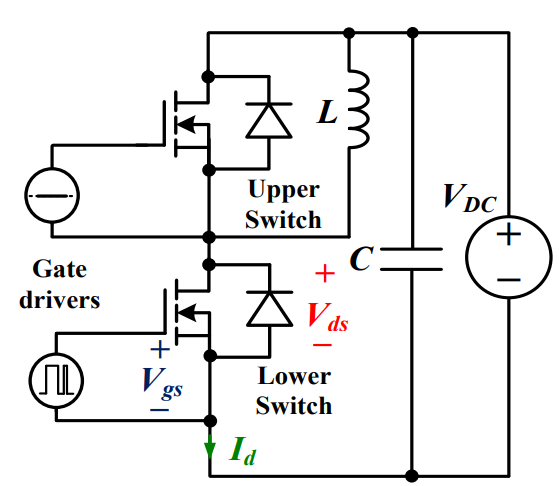 Discovering New and Advanced Methodology for Determining the Dynamic Characterization of Wide Bandgap DevicesSaumitra Jagdale15 March 20242914
For a long era, silicon has stood out as the primary material for fabricating electronic devices due to its affordability, moderate efficiency, and performance capabilities. Despite its widespread use, silicon faces several limitations that render it unsuitable for applications involving high power and elevated temperatures. As technological advancements continue and the industry demands enhanced efficiency from devices, these limitations become increasingly vivid. In the quest for electronic devices that are more potent, efficient, and compact, wide bandgap materials are emerging as a dominant player. Their superiority over silicon in crucial aspects such as efficiency, higher junction temperatures, power density, thinner drift regions, and faster switching speeds positions them as the preferred materials for the future of power electronics.
Read More Applications of FPGAs in Artificial Intelligence: A Comprehensive GuideUTMEL29 August 20255688
This comprehensive guide explores FPGAs as powerful AI accelerators that offer distinct advantages over traditional GPUs and CPUs. FPGAs provide reconfigurable hardware that can be customized for specific AI workloads, delivering superior energy efficiency, ultra-low latency, and deterministic performance—particularly valuable for edge AI applications. While GPUs excel at parallel processing for training, FPGAs shine in inference tasks through their adaptability and power optimization. The document covers practical implementation challenges, including development complexity and resource constraints, while highlighting solutions like High-Level Synthesis tools and vendor-specific AI development suites from Intel and AMD/Xilinx. Real-world applications span telecommunications, healthcare, autonomous vehicles, and financial services, demonstrating FPGAs' versatility in mission-critical systems requiring real-time processing and minimal power consumption.
Read More The 2026 Engineer’s Guide: Choosing the Right MCU for Your Next IoT & New Energy ProjectUTMEL30 April 20262043
A comprehensive comparison of 2026's leading MCUs from ST, NXP, and Microchip across power efficiency, processing performance, connectivity, and ecosystems to help engineers select the optimal chip for next-gen IoT and new energy projects.
Read More AI Server Components: Engineering Next-Gen Data Center Hardware for 100kW RacksUTMEL15 May 20261073
The transition from traditional enterprise IT to AI-driven workloads has rendered legacy data center hardware obsolete, forcing infrastructure planners to re-engineer server components for extreme thermal environments.
Read More The Practical Engineer’s Guide to the NE555N Timer: Pinout, Setup, and TroubleshootingUTMEL29 May 2026921
This comprehensive guide explores the NE555N timer, detailing its 8-pin layout, internal architecture, and key datasheet specifications. It compares the bipolar IC to CMOS variants and details setup configurations for astable, monostable, and bistable modes. Additionally, the guide offers practical troubleshooting advice to prevent common breadboard failures, such as floating reset pins and electrical noise issues.
Read More
Subscribe to Utmel !
![AT88SC3216C-PU]() AT88SC3216C-PU
AT88SC3216C-PUMicrochip Technology
![AT88SA10HS-TSU-T]() AT88SA10HS-TSU-T
AT88SA10HS-TSU-TMicrochip Technology
![HCPL-3020-000E]() HCPL-3020-000E
HCPL-3020-000EBroadcom Limited
![HCPL-3020-500E]() HCPL-3020-500E
HCPL-3020-500EBroadcom Limited
![ATECC608A-SSHCZ-T]() ATECC608A-SSHCZ-T
ATECC608A-SSHCZ-TMicrochip Technology
![SI8261BAC-C-ISR]() SI8261BAC-C-ISR
SI8261BAC-C-ISRSilicon Labs
![HCPL-314J-000E]() HCPL-314J-000E
HCPL-314J-000EBroadcom Limited
![ADUM4120-1BRIZ]() ADUM4120-1BRIZ
ADUM4120-1BRIZAnalog Devices Inc.
![ADUM7223ACCZ]() ADUM7223ACCZ
ADUM7223ACCZAnalog Devices Inc.
![DLPA1000YFFT]() DLPA1000YFFT
DLPA1000YFFTTexas Instruments


